Analog

How to generate sin and cos waves using the LECD PWM on the STM32

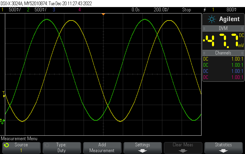
Based on our previous post How to generate PWM output representing a sine wave on the ESP32 (Arduino/PlatformIO) this post uses two different IO pins to generate both a sine and a cosine wave dynamically.

#include <Arduino.h>
#include <driver/ledc.h>

void setup() {
    Serial.begin(115200);

    ledcSetup(LEDC_CHANNEL_0, 10000 /* Hz */, 12);
    ledcSetup(LEDC_CHANNEL_1, 10000 /* Hz */, 12);

    ledcAttachPin(GPIO_NUM_32, LEDC_CHANNEL_0);
    ledcAttachPin(GPIO_NUM_25, LEDC_CHANNEL_1);
}

/**
 * @brief Calculate the PWM duty cycle (assuming 12 bits resolution) of a sine wave of
 * given frequency. micros() is used as a timebase
 * 
 * @param frequency The frequency in Hz
 * @return int the corresponding 12-bit PWM value
 */
int sinePWMValue(float frequency, int maxPWMValue, float (*sinCos)(float)) {
  unsigned long currentMicros = micros(); // get the current time in microseconds

  // calculate the sine wave value for the current time
  int halfMax = maxPWMValue/2;
  int sineValue = halfMax + (halfMax-10) * sinCos(2 * PI * currentMicros / (1000000 / frequency));
  return sineValue;
}

void loop() {
    // Example of how to change the duty cycle to 25%
    ledcWrite(LEDC_CHANNEL_0, sinePWMValue(1.0, 4096, sinf));
    ledcWrite(LEDC_CHANNEL_1, sinePWMValue(1.0, 4096, cosf));
}

The output, filtered by a 4th order Salley-Key filter each (using the LM324) looks like this:

Posted by Uli Köhler in Analog, Arduino, Electronics, ESP8266/ESP32, PlatformIO

What are the ESP32 DAC output pins?

  • Pin IO25 is connected to DAC_1
  • Pin IO26 is connected to DAC_2

Source: ESP32 technical reference manual, Table 4-4

Posted by Uli Köhler in Analog, ESP8266/ESP32

How to turn DL3021 off via SCPI/LXI

In order to turn off the DL3021 electronic load (as in: disable any constant current/resistance/voltage/power function) via LXI, run the following command:

:SOURCE:INPUT:STATE Off

PyVISA example

For more info, see PyVISA Rigol DL3021 via LXI (TCP SCPI) example

#!/usr/bin/env python3

rm = pyvisa.ResourceManager()
inst = rm.open_resource("TCPIP0::192.168.178.112::INSTR")
# Query if instrument is present
# Prints e.g. "RIGOL TECHNOLOGIES,DL3021,DL3A204800938,00.01.05.00.01"
print(inst.query("*IDN?"))

# Turn electronic load off
inst.write(":SOURCE:INPUT:STATE Off")


Posted by Uli Köhler in Analog, Electronics, Networking, Python

Simple OpAmp selectable gain amplifier: Select gain 1x or 10x via GPIO

Download KiCAD 6.x Selectable gain amplifier schematic SGA.kicad_sch

This circuit is a simple variant of a selectable gain amplifier.

If CTRL is pulled low (i.e. to GND), effectively the circuit will look like this:

Due to negligible input bias current for JFET opamps like the TL084 (i.e. most modern opamps below 100 MHz GBW), this circuit is basically just a Gain 1 buffer.

If CTRL is pulled high (i.e. pulled to 5V for example), the circuit effectively looks like this:


which has a gain of (\frac{10 k\Omega}{10 k\Omega + 90 k\Omega} = \frac{10 k\Omega}{100 k\Omega} = 10. Adjust these

One aspect to consider here is the RDSon of the MOSFET Q1. This is added to R1 and introduces a gain error to the system. The BSS123, for example, has a relatively high RDSon of up to 10 Ohms at VGS = 4.5V. For R1 = 10kOhm, the effective worst-case gain is:

\frac{10 k\Omega + 10 \Omega}{10 k\Omega + 10 \Omega + 90 k\Omega} = \frac{10 k\Omega}{100 k\Omega} = 10.001  or 0.01%. For most applications this does not matter since other aspects like the resistnance tolerance or resistance coefficient of temperature will affect the system error orders of magnitude This gain error will vary with temperature since the RDSon is temperature-sensitive and often the variation will be a larger issue than the gain error itself.

One way to mitigate is to choose large values for R1 and R2. Choosing R1=100kOhm and R2=900kOhm in this example will reduce both the gain error and the gain error temperature coefficient from the RDSon of Q1 by an order of magnitude. I recommend not to choose resistors larger than 1 MOhm without taking further consideration of opamp bias current, bias current temperatur drift etc, since those start to get relevant even for JFET input opamps when exceeding a couple of Megaohms.

Note that the RDSon of the MOSFET will be worse for VGS=3.3V will be worse and some MOSFETs will not switch on properly at this voltage. Choose a MOSFET that fits both your logic voltage and the RDSon i.e. gain error requirements. I often start with the BSS138 since I have many of those in stock, which tends to have less than 1 Ohm resistance in most practical conditions.

Another consideration for this circuit is that the MOSFET body diode will conduct if the voltage at the inverting input of the opamp will go beyond the Vf of the MOSFET body diode (typically you should use 0.7V here even if the specified body diode voltage is slightly higher, in order to have sufficient headroom). In effect, this typically means that you should not use this circuit without modification when using bipolar supplies and signals that go more negative than GND.

Posted by Uli Köhler in Analog, Electronics