KiCAD

How to read KiCAD pick&place position file using pandas in Python

If you’ve exported a KiCAD pick & place position file using the GUI or the command line:

kicad-cli pcb export pos MyPCB.kicad_pcb --units mm -o MyPCB.pos

you can read it from within your Python script using pandas.read_table(...) like this:

import pandas as pd

pos = pd.read_table('KKS-Microcontroller-Board-R2.2.pos', delim_whitespace=True, names=["Ref", "Val", "Package", "PosX", "PosY", "Rot","Side"], comment="#")

Optionally, you can also index pos by the Ref column (which contains values such as C12D1 or U5):

pos.set_index("Ref", inplace=True)

You can also pack all that into a function:

def read_kicad_pos_file(filename):
    pos = pd.read_table(filename, delim_whitespace=True, names=["Ref", "Val", "Package", "PosX", "PosY", "Rot","Side"], comment="#")
    pos.set_index("Ref", inplace=True)
    return pos

If you’ve used .set_index(), you can access a component such as C13 using

pos.loc["C13"]

Example output:

Val                100nF_25V
Package    C_0603_1608Metric
PosX                187.1472
PosY               -101.8243
Rot                    180.0
Side                     top
Name: C1, dtype: object


Posted by Uli Köhler in KiCAD, pandas, Python

How to export KiCAD pick&place position file using kicad-cli

Since KiCAD 7.0, you can use the kicad-cli command line tool to export a pick & place position TSV file from a KiCAD project.

First, find out what the filename of the PCB file is. Typically, if your project is named MyPCB.kicad_pro, your main schematic file is named MyPCB.kicad_pcb.

Now you can export the position file using

kicad-cli pcb export pos MyPCB.kicad_pcb --units mm

This will output, for example

Loading board

If the PCB file is named MyPCB.kicad_pcb, the position file will be called MyPCB.pos.

You can also set a custom output file name such as out.pos using the -o option.

kicad-cli pcb export pos MyPCB.kicad_pcb -o out.pos --units mm


Posted by Uli Köhler in KiCAD

How to export KiCAD schematic PDF using kicad-cli

Since KiCAD 7.0, you can use the kicad-cli command line tool to export a colored schematic PDF from a KiCAD project.

First, find out what the filename of the main schematic file is. Typically, if your project is named MyPCB.kicad_pro, your main schematic file is named MyPCB.kicad_sch.

Now you can export the schematic PDF using

kicad-cli sch export pdf MyPCB.kicad_sch

This will output, for example

Plotted to '/home/uli/MyPCB/MyPCB.pdf'.

Done.

The PDF file from the output contains your schematic PDF.

Posted by Uli Köhler in KiCAD

How to get footprint graphical elements using KiCAD pcbnew plugin Python API

See our previous post How to get list of all footprints using KiCAD pcbnew plugin Python API and How to get all selected footprints using KiCAD pcbnew plugin Python API for more info on how to obtain a footprint object.

Once you have a pcbnew.FOOTPRINT object, you can get its graphical elements (which are basically the lines, rectangles, circles etc in the footprint – but not any silkscreen labels) using

footprint.GraphicalElements()

Example:

for graphical_element in footprint.GraphicalItems():   
    print(graphical_element)

Output:

<pcbnew.FP_TEXT; proxy of <Swig Object of type 'FP_TEXT *' at 0x7fc47f2c41e0> >
<pcbnew.FP_SHAPE; proxy of <Swig Object of type 'FP_SHAPE *' at 0x7fc47f0f10b0> >
<pcbnew.FP_SHAPE; proxy of <Swig Object of type 'FP_SHAPE *' at 0x7fc47f2c69d0> >
<pcbnew.FP_SHAPE; proxy of <Swig Object of type 'FP_SHAPE *' at 0x7fc47f2c6d30> >
<pcbnew.FP_SHAPE; proxy of <Swig Object of type 'FP_SHAPE *' at 0x7fc47f0f10e0> >
<pcbnew.FP_SHAPE; proxy of <Swig Object of type 'FP_SHAPE *' at 0x7fc47f2c6cd0> >
<pcbnew.FP_SHAPE; proxy of <Swig Object of type 'FP_SHAPE *' at 0x7fc47f2c6ca0> >
<pcbnew.FP_SHAPE; proxy of <Swig Object of type 'FP_SHAPE *' at 0x7fc47f0f38d0> >
<pcbnew.FP_SHAPE; proxy of <Swig Object of type 'FP_SHAPE *' at 0x7fc47f2c68b0> >
<pcbnew.FP_SHAPE; proxy of <Swig Object of type 'FP_SHAPE *' at 0x7fc47f2c41e0> >
<pcbnew.FP_SHAPE; proxy of <Swig Object of type 'FP_SHAPE *' at 0x7fc47f0f10b0> >
<pcbnew.FP_SHAPE; proxy of <Swig Object of type 'FP_SHAPE *' at 0x7fc47f2c69d0> >
<pcbnew.FP_SHAPE; proxy of <Swig Object of type 'FP_SHAPE *' at 0x7fc47f2c6d30> >

You can filter them using

fp_texts: list[pcbnew.FP_TEXT] = [
    item for footprint in selected_footprint.GraphicalItems()
    if type(item).__name__ == 'FP_TEXT'
]
fp_shapes: list[pcbnew.FP_SHAPE] = [
    item for footprint in selected_footprint.GraphicalItems()
    if type(item).__name__ == 'FP_SHAPE'
]


Posted by Uli Köhler in Electronics, KiCAD

How to get all selected footprints using KiCAD pcbnew plugin Python API

In our previous post, we showed how to get all selected objects using the KiCAD python API using

pcbnew.GetCurrentSelection()

You can simply filter these entries to obtain just a list of selected footprints using either a for loop with inline filtering:

for selected_object in pcbnew.GetCurrentSelection():
    if type(selected_object).__name__ == 'FOOTPRINT':
        print(selected_object.GetReference())

or using a list comprehension:

selected_footprints: list[pcbnew.FOOTPRINT] = [
    footprint for footprint in pcbnew.GetCurrentSelection() if type(footprint).__name__ == 'FOOTPRINT'
]

Complete plugin example:

#!/usr/bin/env python
import pcbnew
import os

class SimplePlugin(pcbnew.ActionPlugin):
    def defaults(self):
        self.name = "Plugin Name as shown in Pcbnew: Tools->External Plugins"
        self.category = "A descriptive category name"
        self.description = "A description of the plugin and what it does"
        self.show_toolbar_button = False # Optional, defaults to False
        self.icon_file_name = os.path.join(os.path.dirname(__file__), 'simple_plugin.png') # Optional, defaults to ""

    def Run(self):
        board: pcbnew.BOARD = pcbnew.GetBoard()
        footprints: list[pcbnew.FOOTPRINT] = board.GetFootprints()
        
        # TODO Do something useful with [board]
        for selected_object in pcbnew.GetCurrentSelection():
            print(selected_object)

SimplePlugin().register() # Instantiate and register to Pcbnew

Example output (excerpt):

D39
D32
D23
D37
D18
D34
D11
D15


Posted by Uli Köhler in Electronics, KiCAD

How to get all selected objects using KiCAD pcbnew plugin Python API

When you have a FOOTPRINT object or a list of footprints in KiCAD’s Python API such as from board.GetFootprints(), you can get their reference designators such as C11 or R4 using

pcbnew.GetCurrentSelection():

Not that not only footprints might be selected but also other objects such as shapes, vias, pads etc.

Complete plugin example:

#!/usr/bin/env python
import pcbnew
import os

class SimplePlugin(pcbnew.ActionPlugin):
    def defaults(self):
        self.name = "Plugin Name as shown in Pcbnew: Tools->External Plugins"
        self.category = "A descriptive category name"
        self.description = "A description of the plugin and what it does"
        self.show_toolbar_button = False # Optional, defaults to False
        self.icon_file_name = os.path.join(os.path.dirname(__file__), 'simple_plugin.png') # Optional, defaults to ""

    def Run(self):
        board: pcbnew.BOARD = pcbnew.GetBoard()
        footprints: list[pcbnew.FOOTPRINT] = board.GetFootprints()
        
        for selected_object in pcbnew.GetCurrentSelection():
            # TODO Do something useful with selected_object
            print(selected_object)

SimplePlugin().register() # Instantiate and register to Pcbnew

Example output (excerpt):

<pcbnew.PCB_VIA; proxy of <Swig Object of type 'PCB_VIA *' at 0x7fc49d2a8b70> >
<pcbnew.PCB_TRACK; proxy of <Swig Object of type 'PCB_TRACK *' at 0x7fc49d2a8de0> >
<pcbnew.PCB_TRACK; proxy of <Swig Object of type 'PCB_TRACK *' at 0x7fc49d2a8c30> >
<pcbnew.PCB_TRACK; proxy of <Swig Object of type 'PCB_TRACK *' at 0x7fc49d2a8b40> >
<pcbnew.PCB_TRACK; proxy of <Swig Object of type 'PCB_TRACK *' at 0x7fc49d2a8db0> >
<pcbnew.PCB_TRACK; proxy of <Swig Object of type 'PCB_TRACK *' at 0x7fc49d2a8c00> >
<pcbnew.PCB_TRACK; proxy of <Swig Object of type 'PCB_TRACK *' at 0x7fc49d2a8ba0> >
<pcbnew.PCB_VIA; proxy of <Swig Object of type 'PCB_VIA *' at 0x7fc49d2a8e10> >
<pcbnew.PCB_VIA; proxy of <Swig Object of type 'PCB_VIA *' at 0x7fc49d2a8bd0> >
<pcbnew.PCB_TRACK; proxy of <Swig Object of type 'PCB_TRACK *' at 0x7fc49d2a8b70> >
<pcbnew.PCB_TRACK; proxy of <Swig Object of type 'PCB_TRACK *' at 0x7fc49d2a8de0> >
<pcbnew.PCB_TRACK; proxy of <Swig Object of type 'PCB_TRACK *' at 0x7fc49d2a8c30> >
<pcbnew.PCB_TRACK; proxy of <Swig Object of type 'PCB_TRACK *' at 0x7fc49d2a8b40> >
<pcbnew.FOOTPRINT; proxy of <Swig Object of type 'std::deque< FOOTPRINT * >::value_type' at 0x7fc49d2a8db0> >
<pcbnew.FOOTPRINT; proxy of <Swig Object of type 'std::deque< FOOTPRINT * >::value_type' at 0x7fc49d2a8c00> >
<pcbnew.FOOTPRINT; proxy of <Swig Object of type 'std::deque< FOOTPRINT * >::value_type' at 0x7fc49d2a8ba0> >
<pcbnew.PCB_VIA; proxy of <Swig Object of type 'PCB_VIA *' at 0x7fc49d2a8e10> >
<pcbnew.PCB_VIA; proxy of <Swig Object of type 'PCB_VIA *' at 0x7fc49d2a8bd0> >
<pcbnew.FOOTPRINT; proxy of <Swig Object of type 'std::deque< FOOTPRINT * >::value_type' at 0x7fc49d2a8b70> >
<pcbnew.FOOTPRINT; proxy of <Swig Object of type 'std::deque< FOOTPRINT * >::value_type' at 0x7fc49d2a8de0> >
<pcbnew.PCB_TRACK; proxy of <Swig Object of type 'PCB_TRACK *' at 0x7fc49d2a8c30> >
<pcbnew.PCB_TRACK; proxy of <Swig Object of type 'PCB_TRACK *' at 0x7fc49d2a8b40> >
<pcbnew.FOOTPRINT; proxy of <Swig Object of type 'std::deque< FOOTPRINT * >::value_type' at 0x7fc49d2a8db0> >
<pcbnew.PCB_VIA; proxy of <Swig Object of type 'PCB_VIA *' at 0x7fc49d2a8c00> >
<pcbnew.FOOTPRINT; proxy of <Swig Object of type 'std::deque< FOOTPRINT * >::value_type' at 0x7fc49d2a8ba0> >
<pcbnew.FOOTPRINT; proxy of <Swig Object of type 'std::deque< FOOTPRINT * >::value_type' at 0x7fc49d2a8e10> >
<pcbnew.FOOTPRINT; proxy of <Swig Object of type 'std::deque< FOOTPRINT * >::value_type' at 0x7fc49d2a8bd0> >
<pcbnew.FOOTPRINT; proxy of <Swig Object of type 'std::deque< FOOTPRINT * >::value_type' at 0x7fc49d2a8b70> >
<pcbnew.PCB_TRACK; proxy of <Swig Object of type 'PCB_TRACK *' at 0x7fc49d2a8de0> >
<pcbnew.FOOTPRINT; proxy of <Swig Object of type 'std::deque< FOOTPRINT * >::value_type' at 0x7fc49d2a8c30> >
<pcbnew.PCB_TRACK; proxy of <Swig Object of type 'PCB_TRACK *' at 0x7fc49d2a8b40> >
<pcbnew.PCB_VIA; proxy of <Swig Object of type 'PCB_VIA *' at 0x7fc49d2a8db0> >
<pcbnew.PCB_TRACK; proxy of <Swig Object of type 'PCB_TRACK *' at 0x7fc49d2a8c00> >
<pcbnew.PCB_TRACK; proxy of <Swig Object of type 'PCB_TRACK *' at 0x7fc49d2a8ba0> >
<pcbnew.FOOTPRINT; proxy of <Swig Object of type 'std::deque< FOOTPRINT * >::value_type' at 0x7fc49d2a8e10> >
<pcbnew.FOOTPRINT; proxy of <Swig Object of type 'std::deque< FOOTPRINT * >::value_type' at 0x7fc49d2a8bd0> >
<pcbnew.PCB_VIA; proxy of <Swig Object of type 'PCB_VIA *' at 0x7fc49d2a8b70> >


Posted by Uli Köhler in Electronics, KiCAD

How to get list footprint Reference Designators KiCAD pcbnew plugin Python API

When you have a FOOTPRINT object or a list of footprints in KiCAD’s Python API such as from board.GetFootprints(), you can get their reference designators such as C11 or R4 using

footprint.GetReference()

Complete plugin example:

#!/usr/bin/env python
import pcbnew
import os

class SimplePlugin(pcbnew.ActionPlugin):
    def defaults(self):
        self.name = "Plugin Name as shown in Pcbnew: Tools->External Plugins"
        self.category = "A descriptive category name"
        self.description = "A description of the plugin and what it does"
        self.show_toolbar_button = False # Optional, defaults to False
        self.icon_file_name = os.path.join(os.path.dirname(__file__), 'simple_plugin.png') # Optional, defaults to ""

    def Run(self):
        board: pcbnew.BOARD = pcbnew.GetBoard()
        footprints: list[pcbnew.FOOTPRINT] = board.GetFootprints()
        
        # TODO Do something useful with [board]
        for footprint in footprints:
            print(footprint.GetReference())

SimplePlugin().register() # Instantiate and register to Pcbnew


Posted by Uli Köhler in Electronics, KiCAD

How to get list of all footprints using KiCAD pcbnew plugin Python API

When using KiCAD’s Python API for pcbnew, you can obtain a list of FOOTPRINTobjects using

board: pcbnew.BOARD = pcbnew.GetBoard()
footprints: list[pcbnew.FOOTPRINT] = board.GetFootprints()

The : pcbnew.BOARD and : list[pcbnew.FOOTPRINT] are optional but will tell your editor (such as visual studio code) which object to expect for better autocompletion.

Complete plugin example:

#!/usr/bin/env python
import pcbnew
import os

class SimplePlugin(pcbnew.ActionPlugin):
    def defaults(self):
        self.name = "Plugin Name as shown in Pcbnew: Tools->External Plugins"
        self.category = "A descriptive category name"
        self.description = "A description of the plugin and what it does"
        self.show_toolbar_button = False # Optional, defaults to False
        self.icon_file_name = os.path.join(os.path.dirname(__file__), 'simple_plugin.png') # Optional, defaults to ""

    def Run(self):
        board: pcbnew.BOARD = pcbnew.GetBoard()
        footprints: list[pcbnew.FOOTPRINT] = board.GetFootprints()
        
        # TODO Do something useful with [board]
        for footprint in footprints:
            print(footprint)

SimplePlugin().register() # Instantiate and register to Pcbnew


Posted by Uli Köhler in Electronics, KiCAD

How to get board object using KiCAD pcbnew plugin Python API

When using KiCAD’s Python API for pcbnew, you can simply get a board object using pcbnew.GetBoard():

board: pcbnew.BOARD = pcbnew.GetBoard()

The : pcbnew.BOARD is optional but will tell your editor (such as visual studio code) which object to expect for better autocompletion.

Complete plugin example:

#!/usr/bin/env python
import pcbnew
import os

class SimplePlugin(pcbnew.ActionPlugin):
    def defaults(self):
        self.name = "Plugin Name as shown in Pcbnew: Tools->External Plugins"
        self.category = "A descriptive category name"
        self.description = "A description of the plugin and what it does"
        self.show_toolbar_button = False # Optional, defaults to False
        self.icon_file_name = os.path.join(os.path.dirname(__file__), 'simple_plugin.png') # Optional, defaults to ""

    def Run(self):
        board: pcbnew.BOARD = pcbnew.GetBoard()
        # TODO Do something useful with [board]
        print(board)

SimplePlugin().register() # Instantiate and register to Pcbnew


Posted by Uli Köhler in Electronics, KiCAD

How to fix KiCAD JLCPCB fabrication plugin error: The wx.App object must be created first!

Problem:

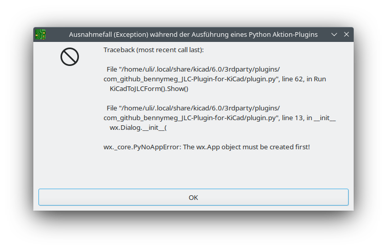
When running the JLCPCB fabrication plugin in KiCAD to export fabrication data, you see the following error message:

wx._core.PyNoAppError: The wx.App object must be created first!

Solution:

This appears to be a bug with current versions of the JLCPCB fabrication plugin, but you can easily fix it by adding a line to plugin.py, which is located here:

/home/uli/.local/share/kicad/6.0/3rdparty/plugins/com_github_bennymeg_JLC-Plugin-for-KiCad/plugin.py

(depending on the operating system, the kicad folder will be located elsewhere).

Find the following lines which are almost at the top of the file:

# WX GUI form that show the plugin progress
class KiCadToJLCForm(wx.Frame):
    def __init__(self):

and add the following line directly after def __init__(self):

        self.app = wx.PySimpleApp()

Result:

# WX GUI form that show the plugin progress
class KiCadToJLCForm(wx.Frame):
    def __init__(self):
        self.app = wx.PySimpleApp()


Posted by Uli Köhler in KiCAD

Selectable 3.3V / 5V / 12V supply (with KiCAD schematic)

This example shows you how to make a selectable output voltage (3.3V / 5V / 12V) switching voltage regulator using the AP63200WU (2A current capability – but the approach works with any adjustable voltage regulator). The voltage can be selected using a three-way jumper.

The main trick here is to change the feedback network when selecting the output voltage.

One major mistake is to design the regulator so it doesn’t operate safely when the jumper is removed (for example, the output voltage goes to 12V or even up to the input voltage when no jumper is connected). In our circuit, when no jumper is used, the output voltage is 3.3V. We achieve this by using selectable (& optional) resistors in parallel to the bottom feedback resistor. The 3.3V feedback resistor is fixed.
Using a selectable-in-parallel-to-bottom-FB-resistor topology will always guarantee that the lowest output voltage will be selected when none of the optional parallel resistors are active.

Download this schematic as KiCAD file

Posted by Uli Köhler in Electronics, KiCAD

How to check a KiCAD footprint against KLC (KiCAD library conventions)

First, clone kicad-library-utils using

git clone https://gitlab.com/kicad/libraries/kicad-library-utils.git

Then, run the check script against your footprint – Connector_RJ.pretty/RJ9_Evercom_5301-4P4C.kicad_mod
in this example – using

~/kicad-library-utils/klc-check/check_footprint.py -vv Connector_RJ.pretty/RJ9_Evercom_5301-4P4C.kicad_mod

You might need to adjust the path to kicad-library-utils accordingly.

This will provide colored output on the command line such as

Checking footprint 'RJ9_Evercom_5301-4P4C':
  Violating F5.2 - https://klc.kicad.org/footprint/f5/f5.2/
    Fabrication layer requirements
    Value Label Errors
  Violating F7.2 - https://klc.kicad.org/footprint/f7/f7.2/
    For through-hole components, footprint anchor is set on pad 1
    Pad '1' not located at origin
  Violating F9.1 - https://klc.kicad.org/footprint/f9/f9.1/
    Footprint meta-data is filled in as appropriate
    Value label '5301-4P4C' does not match filename 'RJ9_Evercom_5301-4P4C'
  Violating F9.3 - https://klc.kicad.org/footprint/f9/f9.3/
    Footprint 3D model requirements
    3D model file path missing from the 3D model settings of the footprint


Posted by Uli Köhler in Electronics, KiCAD

Where to find cheap tactile switches / push buttons?

LCSC has a really cheap all-metal push button for only 0.0129€/pc @50pc

HCTL TC-0522C-1.6-160G

Direct datasheet link

It works with the KiCAD 6.0

Button_Switch_SMD:SW_SPST_TL3342

footprint and the KiCAD 6.0

Switch:SW_Push

symbol.

Posted by Uli Köhler in Components, Electronics, KiCAD

Where to find box header footprints in KiCAD?

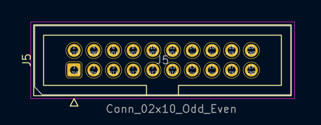
You can find all box headers in the Connector_IDC library in KiCAD. This library is from the standard set of KiCAD libraries, hence you don’t need to install it manually.

Posted by Uli Köhler in KiCAD

How to enable KiCAD snap to pads in measure distance mode

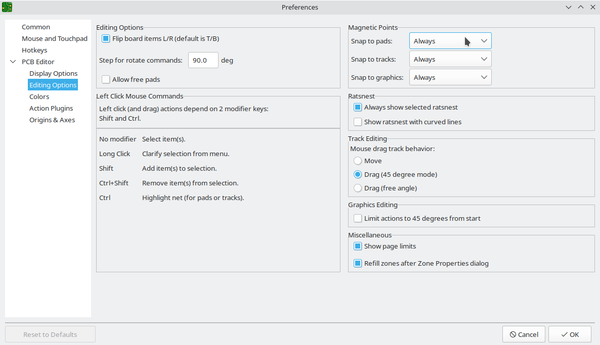
In order to enable snapping to pads (also called magnetic pads) in KiCAD pcbnew, open Preferences -> Preferences:

and then open PCB Editor -> Editing Options, and set Magnetic Points -> Snap to pads to Always:

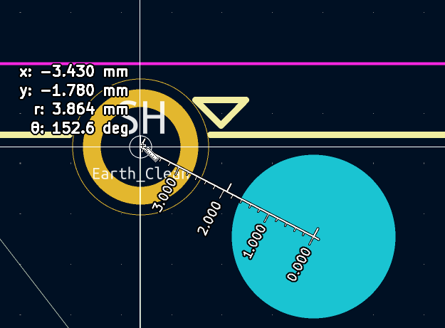
After you click OK, you can snap to points when using the Ctrl+M Interactively measure distance between points tool:

Posted by Uli Köhler in KiCAD

How to connect 100Base-FX transceiver to SFP module (schematic)

Also see my post on selecting a suitable 100Base-FX Ethernet PHY.

Note that sometimes the capacitors and the 100 Ohm termination resistor is integrated in the specific SFP module in use! In that case, replace the capacitors by 0 Ohm resistors and omit the 100 Ohm resistor. My recommendation is to check out the datasheet of the SFP module or just try it out with the capacitors & termination if you don’t know.

100Base-FX transceivers are pretty easy to connect to the PHY, but you have to terminate the high speed interface correctly. Since PECL logic is used, the termination scheme is somewhat difference.

PECL & AC termination

The first thing is understand is that while all SFP modules are equal (i.e. subject to the SFP multi-source agreement), some are more equal than others.

More specifically, some of them include termination resistors, some of them include AC coupling capacitors, some of them include both and some of them include none. My recommendation is to assume that the SFP module contains both AC coupling caps and the transmit termination, but have spare component footprints in case you need to add them. Similar strategies are recommended

What you absolutely need is:

  • A 50 Ohm differential trace between the SFP and the PHY
  • Some termination scheme on the PHY side
  • You 100% absolutely need to checkout your PHY’s datasheet, or ask the manufacturer for reference schematics!
  • Short traces – the shorter the traces, the less headache you’ll get from debugging. You don’t want more headache than neccessary, believe me.

What you might or might not need, depending on SFP, PHY and board layout is:

  • Additional terminations (if you add those while other termination is already in place, this will approximately half your signal amplitude.
  • AC coupling capacitors (doesn’t hurt all too much to include them even if they are redundant)
  • Pullup resistors for the PHY driver

Variant 1: Microchip

The following information is based on Microchip’s application note for the LAN93xx series. The basic termination strategy is to use a 100R differential transmit termination, included with the note that some transceivers already contain the termination resistor inside them and using an extra termination resistor.

Note that in one of the schematics Microchip swapped the termination resistors. The 130 Ohm resistor should go toward 3.3V and not toward ground.

Furthermore, Microchip requires 50 Ohm (read: 49.9 Ohm) pull-up resistors to be fitted to the transmit lines. These resistors are required for the Microchip drivers, but not required for all drivers.

Variant 2: Marvell

In Marvell’s 88E3015/88E3018 datasheet, a slightly different termination scheme is implemented which omits the differential 100R termination resistor in favour of a pair of

Note that the Marvell device does not specify 50R pullup resistors. As far as I could find out SFP modules never appear to require these pullups, but some PHYs do. The only safe variant is to include these pullups into the schematic and do not populated them.

Combining the variants

A good idea with high speed signals, especially with different transceivers is to include all possible options and then just try out what works best.

Download KiCAD schematic

My recommendations on what to start with are as follows:

  • All resistors shown with NA values: Do not populate, populate only if needed experimentally
  • Since most SFP receivers already include AC coupling capacitors, these are not needed, but they typically do not hurt either
  • Try to keep the traces between the PHY and the SFP module short. This will solve most signal integrity problems without having to test-fit resistors etc.

In addition to the high speed data connection from the SFP module to the PHY, you want to find the LOS (loss of signal) pin, sometimes called signal detect or link detect and also connect it directly from the SFP module to the PHY (no termination or pullups required).

Regarding the layout, as usual with high speed connections, ensure that the components are placed near to the relevant components and try to place the PHY and the SFP module as close together as possible.
Posted by Uli Köhler in Electronics, KiCAD, Networking

How to initialize your KiCAD 6 project on the command line

For the KiCAD 5 version of this script see How to initialize your KiCAD 5 project on the command line

TL;DR:

Inside the directory where you want to create the project, run

wget -qO- https://techoverflow.net/scripts/kicad6-init.sh | bash /dev/stdin MyProject

You should replace MyProject (at the end of the command) with your project name.

Note: This will initialize an empty KiCAD project without any libraries. This is equivalent to creating a new project in KiCAD itself (using the GUI).

Continue reading →

Posted by Uli Köhler in Electronics, KiCAD, Shell

How to fix KiBot ‘KiBoM not installed or too old’

Problem:

When running kibot-check, you see the following warning message:

* KiBoM not installed or too old
  Visit: https://github.com/INTI-CMNB/KiBoM
  Download it from: https://github.com/INTI-CMNB/KiBoM/releases
  - Mandatory for `kibom`

but even installing kibom using pip install kibom, the warning does not disappear.

Solution:

You need to install a specific fork of KiBom:

pip install git+https://github.com/INTI-CMNB/KiBoM

After that, the warning will disappear.

Posted by Uli Köhler in Electronics, KiCAD, Python

How to check only a single schematic symbol against KLC (KiCAD library conventions)

In our previous post How to check KiCAD symbol library against KLC (KiCAD library conventions) we showed how to use check_symbol.py to check a symbol library against the KiCAD library guidelines.

You can also use it to check only a specific symbol in that library by name, which removes most of the clutter from the output. Use -c "CD4066B" to just check the component named CD4066B.

~/kicad-library-utils/klc-check/check_symbol.py MyLibrary.kicad_sym -vv -c "CD4066B"

This will print, for example:

Checking symbol 'Analog_Switch:CD4066B':
  Violating S3.1
    Origin is centered on the middle of the symbol
    Symbol unit 3 slightly off-center
     -   Center calculated @ (-25, -25)
    Symbol unit 4 slightly off-center
     -   Center calculated @ (-25, -25)
    Symbol unit 5 not centered on origin
     - Center calculated @ (-100, 0)
  Violating S4.1
    General pin requirements
    Pins not located on 100mil (=2.54mm) grid:
     - Pin C (6) @ (-400,50) 
     - Pin C2 (9) @ (350,-100) 
     - Pin D2 (10) @ (350,-100) 
     - Pin D (12) @ (-400,50) 
  Violating S5.2
    Footprint filters should match all appropriate footprints
    No footprint filters defined


Posted by Uli Köhler in Electronics, KiCAD

How to check KiCAD symbol library against KLC (KiCAD library conventions)

First, clone kicad-library-utils using

git clone https://gitlab.com/kicad/libraries/kicad-library-utils.git

Then, run the check script against your library using

~/kicad-library-utils/klc-check/check_symbol.py MyLibrary.kicad_sym -vv

You might need to adjust the path to kicad-library-utils accordingly.

This will provide colored output on the command line such as

Checking symbol 'Analog_Switch:FSA3157L6X':
Checking symbol 'Analog_Switch:NC7SB3157P6X':
  Violating S3.1
    Origin is centered on the middle of the symbol
    Symbol unit 1 not centered on origin
     - Center calculated @ (0, -112)
  Violating S3.6
    Pin name position offset
    Pin offset outside allowed range
     - Pin offset (5) should not be below 20mils


Posted by Uli Köhler in Electronics, KiCAD